WTF are FPGAs: A Beginner's Overview of Field-Programmable Gate Arrays
If you hang around electronics forums long enough, someone will eventually ask whether they should use a microcontroller or an FPGA for their project. The question itself reveals a misunderstanding. FPGAs do not compete with microcontrollers. They occupy a different region of the design space entirely, and conflating them obscures what makes each tool genuinely useful.
This article is a ground-up introduction to what FPGAs actually are, where they come from, what lives inside them, and what it takes to put one to work.
A Brief History: From 74-Series to Field-Programmable
When I started building digital circuits in the mid-nineties, the standard approach was to wire up 74-series logic ICs on a breadboard. These are small, cheap packages, each containing a handful of logic gates: AND, OR, NAND, NOR, flip-flops, latches, multiplexers, and hundreds of other building blocks. With enough of them you can build anything. Ben Eater’s 8-bit breadboard CPU series is the best demonstration of this I know of: a fully functional processor assembled from discrete 74-series chips, wire by wire.
The 74-series approach has three practical problems:
- Cost and sourcing. You need a lot of parts. Each chip costs a little, but a complex design needs dozens of them, and they all have to be in stock.
- Space and wiring. A breadboard fills up fast. Long wire runs between chips make debugging painful and layouts fragile.
- Signal integrity at high frequencies. Every wire between chips is a small antenna. At high clock rates, propagation delays and reflections from the physical interconnects become a serious problem.
A middle ground emerged in the form of CPLDs (Complex Programmable Logic Devices), which compressed some of this logic into a single programmable package. CPLDs are worth knowing exist, but we will not go further into them here. What followed CPLDs is the focus of this article.
What Is an FPGA?
FPGA stands for Field-Programmable Gate Array. The name already tells you the core idea: an array of logic gates that can be wired up in the field, meaning after manufacturing, by the engineer using it rather than by the chip foundry.
Instead of buying thirty separate 74-series chips and wiring them together on a breadboard, you buy one FPGA. That single IC contains thousands of configurable logic elements and a programmable interconnect fabric. You decide how they connect. The chip stays the same; the configuration changes.
FPGAs are not new, but they are not ancient either. Xilinx introduced the first commercial FPGA in 1985. That is younger than the personal computer and younger than the 74-series itself. The technology has matured enormously since then, but the fundamental idea has remained constant.
What Lives Inside an FPGA
Here is a simplified mental model. Picture a rectangular grid, thousands of cells arranged in a checkerboard pattern. Each cell contains a small block of configurable logic. Between the cells runs an interconnect fabric, a dense mesh of wires called the routing fabric, which is the technical term for what I will keep calling “highways” because that is exactly what they look like from above.
+-------+     +-------+     +-------+
| LOGIC |--?--| LOGIC |--?--| LOGIC |
+-------+     +-------+     +-------+
    |     \  /     |     \  /     |
   ---    ---     ---    ---     ---
    |      |       |      |       |
+-------+     +-------+     +-------+
| LOGIC |--?--| LOGIC |--?--| LOGIC |
+-------+     +-------+     +-------+
    |                              |
   I/O                            I/O
Each logic cell connects to the routing fabric through a set of transistors. Every one of those transistors has a corresponding address in a block of SRAM on the chip. When you load a configuration into that SRAM, every bit that reads 1 closes its transistor, connecting that logic cell to that wire in the routing fabric. Every bit that reads 0 leaves the connection open.
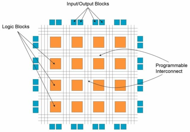
The result: by writing a particular pattern of ones and zeros into the SRAM, you define a complete network of logic gates. Change the pattern, and you define a different network. This is what “field programmable” means in practice.
Because the configuration lives in SRAM, it disappears when power is removed. Most iCE40-based boards (including the iCEstick I used in my VHDL zero-to-one post) work this way: an external SPI flash stores the bitstream and loads it into the FPGA at startup. Some FPGAs integrate the flash on-chip, which simplifies the board design but adds cost. For prototyping and learning, external flash or direct USB programming is the norm.
Logic Cells: Not Quite What the 74-Series Used
Early FPGAs implemented logic cells as collections of primitive gates: AND, OR, NOT. Modern FPGAs typically use Look-Up Tables (LUTs) instead. A LUT is a small block of SRAM that implements any boolean function of N inputs by storing the truth table directly. A 4-input LUT can implement any function of four variables by pre-loading all sixteen output values.
This is a slightly different model from discrete gates, but the abstraction holds: you can still think of each logic cell as a configurable gate. The LUT just makes the implementation more flexible and the area more efficient. For the purposes of understanding what an FPGA is, the “grid of gates connected by programmable highways” model is accurate enough.
Why FPGAs Exist: The Parallelism Argument
A microcontroller executes instructions sequentially. One instruction runs, it finishes, the next one starts. Even with pipelining and multiple cores, there is a fundamental serialization happening at some level.
An FPGA does not execute instructions. It implements circuits. When you configure an FPGA, you describe hardware, not a program. Signal propagation through that hardware happens simultaneously across all configured paths. The time it takes to compute a result depends primarily on how long the signal takes to travel through gates and wires, not on how many other computations are queued up.
This is why FPGAs appear in domains where timing is everything:
- High-frequency trading: decisions made in nanoseconds, not microseconds, can mean the difference between a filled order and a missed one. An FPGA can evaluate market conditions in constant, predictable time.
- Particle physics trigger systems: at facilities like CERN, detectors produce far more data than can be stored or transmitted. FPGAs evaluate trigger conditions in real time and decide within microseconds whether an event is worth recording.
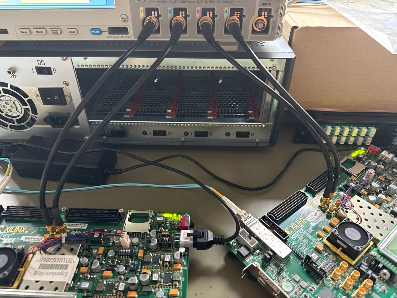
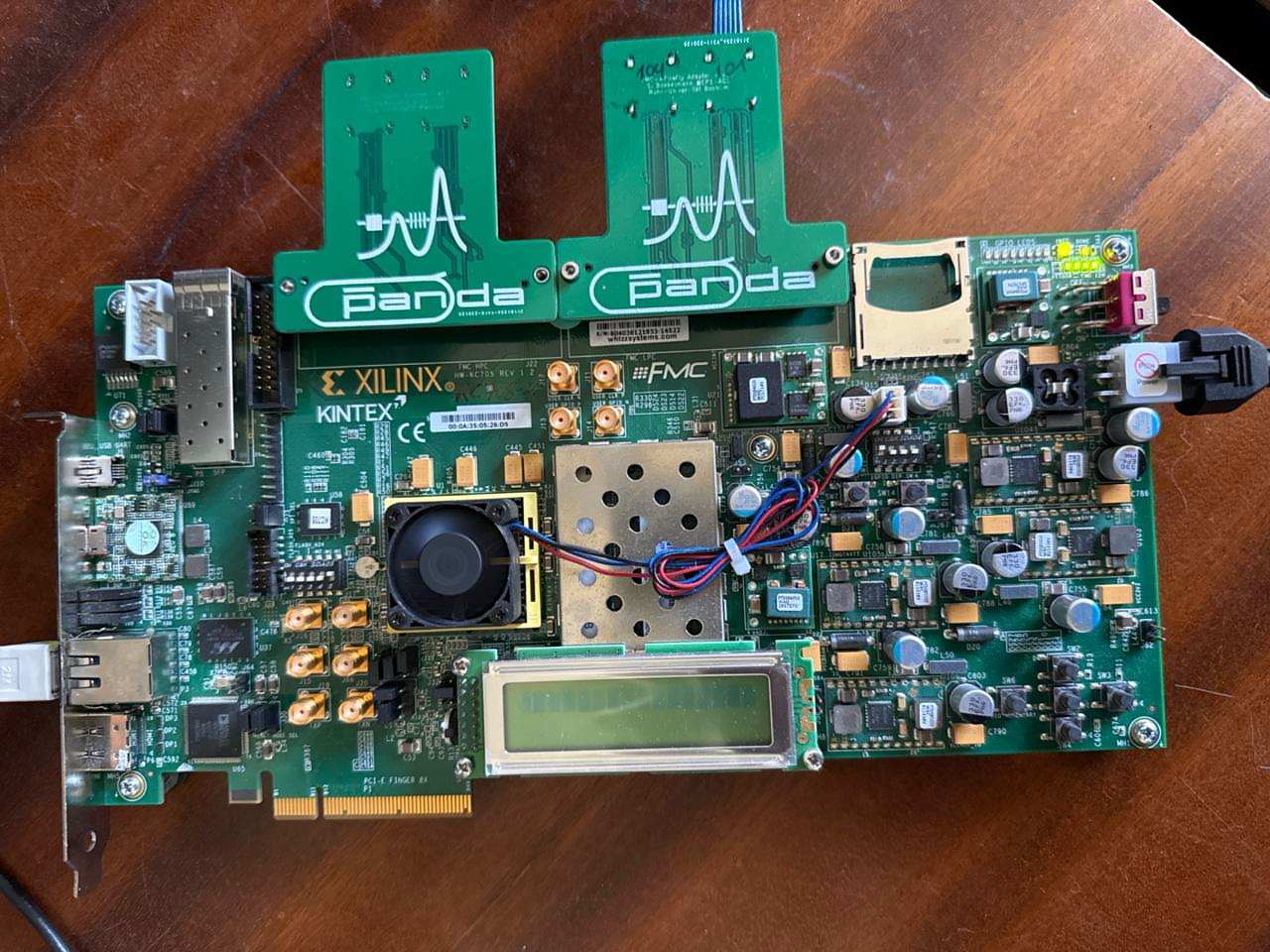
- DAQ systems: data acquisition pipelines that need to handle thousands of parallel analog channels without dropping samples. At EP1 at Ruhr-Universität Bochum, Florian Feldbauer, Niels Boelger, and I use Kintex-7 FPGAs to read out HV-MAPS sensors for the PANDA and LHCb experiments. The boards in the photo below are from exactly that setup.
- Custom processor development: when you are designing a new CPU architecture, an FPGA lets you instantiate your design in real silicon-like hardware before committing to a mask. This is how many research processors are prototyped.
- Cryptography: certain algorithms map extremely efficiently onto parallel hardware. An FPGA can execute specific cryptographic functions with far less energy than a general-purpose CPU or even a GPU, because every gate is doing exactly one useful thing.
None of these use cases require an FPGA to be “better” than a CPU in general. They require it to be different, specifically in how it handles parallelism and timing determinism.
From HDL to Bitstream: The Toolchain
Here is the part that surprises most people when they first encounter FPGAs: getting a design onto a chip is not like flashing firmware. It is a multi-stage engineering process that has more in common with compiling a programming language than with writing a shell script.
Step 1: Describe the Hardware
The starting point is a Hardware Description Language. The two dominant ones are VHDL and Verilog. I prefer VHDL, and I will use it in examples.
A HDL looks like a programming language but is not one. The analogy I find useful: a program is a recipe, and a recipe is not the meal. Similarly, a HDL file is a description of hardware, and that description is not the hardware. A closer analogy is SVG: a text file that describes a graphic, which a renderer then turns into pixels. In the HDL world, the renderer is the synthesis tool.
VHDL and Verilog describe hardware in terms of blocks and signals. A block (called an entity in VHDL or a module in Verilog) defines inputs, outputs, and the logic that maps one to the other. Blocks can be nested and composed, much like components in a schematic. Signals connect blocks together and carry values.
entity blinky is
  port (
    clk : in  std_logic;
    led : out std_logic
  );
end entity;

architecture rtl of blinky is
  signal counter : unsigned(23 downto 0) := (others => '0');
begin
  process(clk)
  begin
    if rising_edge(clk) then
      counter <= counter + 1;
      led <= counter(23);
    end if;
  end process;
end architecture;
This describes a circuit that counts clock edges and drives an LED from the top bit of the counter. There is no main(), no loop, no scheduler. There is a process that responds to a clock signal, and a register that accumulates a value. That is hardware, described as text.
Step 2: Simulate Before You Synthesize
Before touching real silicon, you simulate. A testbench is another VHDL (or Verilog) file that instantiates your design and applies input stimuli with specific timings. A simulator runs the testbench and records how signals change over time.
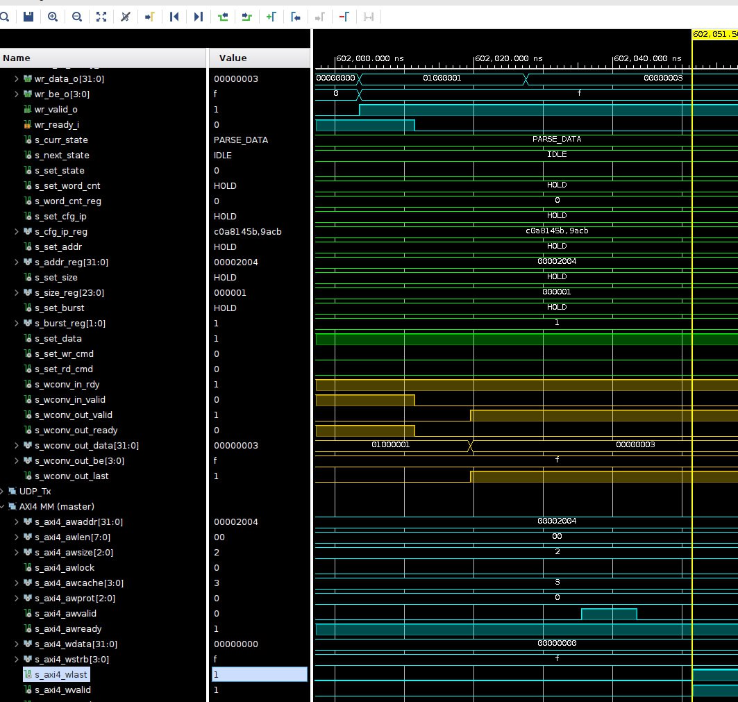
Tools like GTKWave visualize those signal traces, or for Xilinx designs Vivado’s built-in waveform viewer. You can verify that your counter increments correctly, that your state machine reaches the right states, that your UART transmits the right bytes, all without touching a soldering iron.
This step is not optional for serious work. Debugging a circuit in hardware, where you only see what probes you physically attached, is much harder than stepping through a simulation.
Step 3: Synthesize to a Netlist
Once the simulation looks correct, you run synthesis. The synthesis tool (we use yosys for open-source flows, Xilinx’s Vivado for Xilinx FPGAs) reads your HDL and produces a netlist: a hardware-agnostic description of every gate, flip-flop, and connection in your design.
The netlist is technology-independent at this stage. It knows about AND gates and registers, not about the specific resources on any particular FPGA.
Step 4: Place and Route
Now the hardware specifics enter. Every FPGA has a chip description file that maps out exactly which logic cells exist where, how they connect to the routing fabric, and which pins of the package connect to which I/O cells.
You also write a constraint file that maps the logical I/O ports in your design to physical package pins. This is where you say: “the signal I called clk connects to pin 21, which is wired to the 12 MHz oscillator on this board.”
The place-and-route tool (nextpnr in the open-source world) takes the netlist, the chip description, and the constraints, and works out which logic cells to use for each gate in the netlist, and which paths through the routing fabric to use for each signal. For large designs this can take a long time and consume significant memory. The tool is essentially solving a constraint-satisfaction problem over a very large graph.
Step 5: Post-Implementation Simulation
After place and route, modern toolchains can produce a timing-annotated simulation model. This tells you, to nanosecond precision, how long each signal path actually takes to propagate through the routed design on that specific chip. You can run your testbench again against this model and verify that your circuit still behaves correctly when real propagation delays are taken into account.
This is also where hazards show up: transient glitches caused by signals arriving at a gate at slightly different times. We will come back to hazards in a later article.
Step 6: Generate and Load the Bitstream
The final step is bitstream generation. A vendor-specific tool reads the place-and-route output and produces the binary file that programs the FPGA’s configuration SRAM. For the iCE40 family this is done by icepack (part of the icestorm toolchain). For Xilinx parts, Vivado handles this step.
The bitstream is then written to the chip, either directly over USB (as with the iCEstick) or by loading it into external SPI flash so the FPGA configures itself at power-up.
The Form Factors
FPGAs come in a wide range of packages and boards:
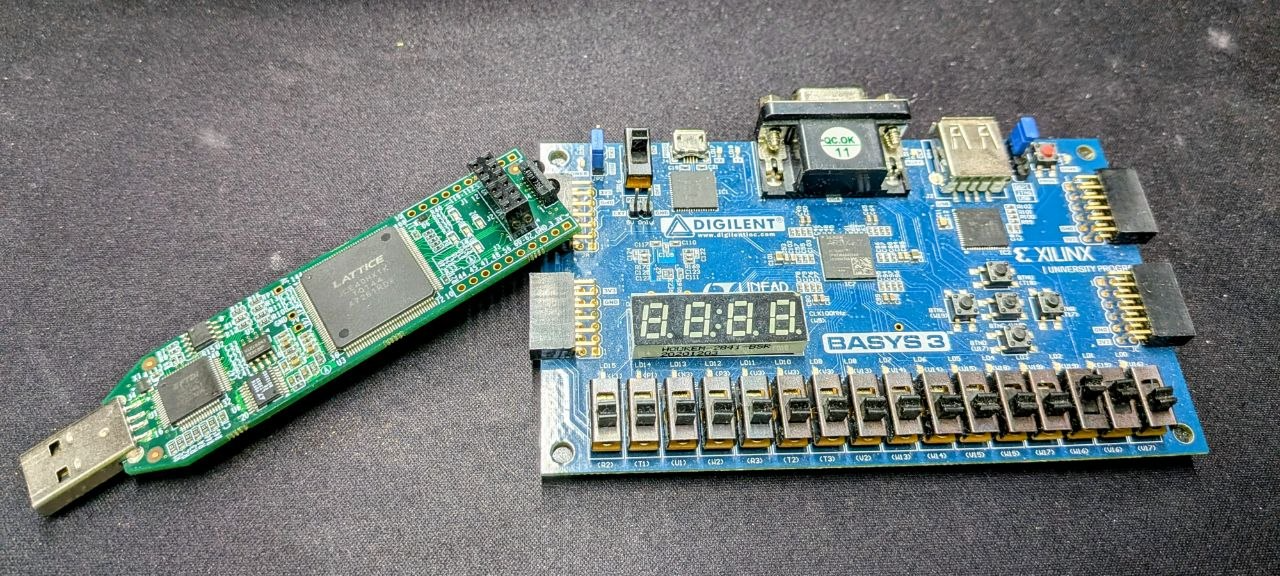
- USB development boards like the Lattice iCEstick: plug into a USB port, fully supported by the open-source icestorm/yosys/nextpnr stack, and cost around 25 euros. The right place to start.
- Larger development boards like the Digilent Nexys or Basys series: more I/O, bigger FPGAs, more on-board peripherals (VGA, audio, switches). A step up once you have outgrown the smaller boards.
- PCIe boards: high-bandwidth FPGAs intended for accelerator workloads, plugged directly into a server’s PCIe bus. Used in HFT, ML inference, and network offload.
The choice of form factor follows from the application. For learning the toolchain, a USB stick is plenty. For a particle physics trigger system, you want something closer to the PCIe end of the spectrum.
FPGAs Are Not Microcontrollers
It is worth saying plainly: an FPGA is not a fast microcontroller, and it is not a replacement for one. A microcontroller runs software. An FPGA implements hardware. The distinction matters.
When you write C for an ATmega, you are telling a CPU what sequence of operations to perform. When you write VHDL for an iCE40, you are describing a circuit that does not have a program counter, does not fetch instructions, and does not wait for a previous operation to finish before starting the next one.
FPGAs expand what is possible in digital design. They do not obsolete anything that came before. A microcontroller is still the right tool for running application logic, talking to sensors, and implementing protocols in software. An FPGA is the right tool when you need parallel, timing-deterministic hardware that does not exist as a standard IC.
The two often appear on the same board, with the microcontroller configuring the FPGA at startup and then sending it commands while the FPGA handles the time-critical path.
Where to Go Next
If you want to put this into practice, the Zero to One: VHDL and a Lattice iCEstick post walks through the full toolchain from a blank editor to a blinking LED on real hardware. Everything described in the toolchain section above becomes concrete there: the VHDL, the testbench, the constraints file, yosys, nextpnr, and the iCEstick.
The FPGA rabbit hole is deep. Signal timing, clock domain crossing, hardware hazards, and advanced synthesis constraints are all topics worth their own articles. This one was about understanding what you are dealing with before you open a terminal.