Zero to One: Fun with SWD
Most embedded tutorials start the same way: install the toolchain, write a main.c, fight the linker script, flash the binary, and then — finally — a LED blinks. That is a perfectly valid path. But there is a shorter one, and it teaches you something the longer path tends to skip: registers are just memory. You can read and write them directly, from your laptop, without compiling anything.
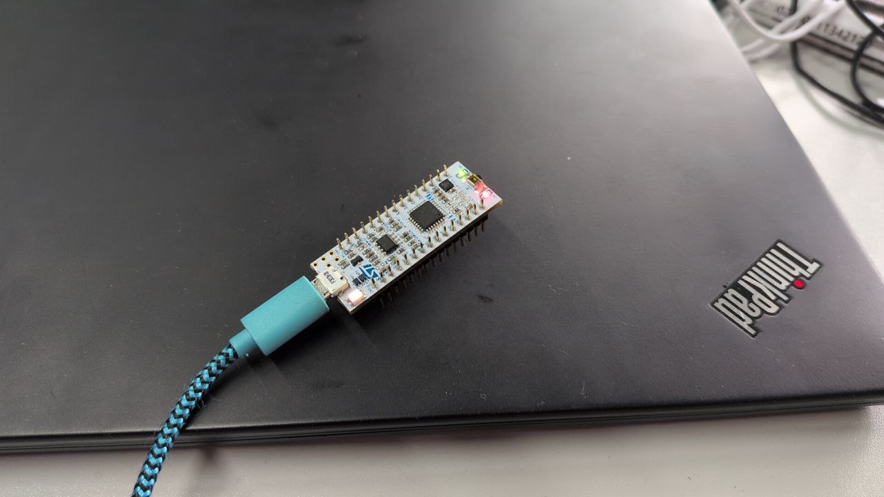
This post shows how to do exactly that on an STM32F303K8 Nucleo-32 using OpenOCD and a plain telnet session.
What Is SWD? Serial Wire Debug Explained
Serial Wire Debug (SWD) is a two-wire protocol — SWDIO (data) and SWDCLK (clock) — defined by ARM for Cortex-M processors. It gives a debug host on your PC read and write access to the entire address space of the microcontroller: Flash, RAM, and every peripheral register.
The ST-Link circuit on the Nucleo board is a USB-to-SWD bridge. When you plug the board into USB your Linux machine sees it as a USB device; OpenOCD speaks to the ST-Link firmware over USB and speaks SWD to the F303 over the two-wire bus.
PC (Linux)
  └── USB ──► ST-Link (onboard)
                └── SWD ──► STM32F303K8
No UART, no bootloader mode, no jumpers to move. The same connection you use to flash firmware is the connection we use here to poke registers live.
Install OpenOCD
On Ubuntu or Debian:
sudo apt update
sudo apt install openocd
Verify the installation:
openocd --version
# Open On-Chip Debugger 0.11.0 (or newer)
udev rules — allow non-root access to the ST-Link
By default, USB devices are owned by root. Without a udev rule you would have to run OpenOCD as root every time. The OpenOCD package ships rules; you just need to activate them:
sudo cp /usr/share/openocd/contrib/60-openocd.rules /etc/udev/rules.d/
sudo udevadm control --reload-rules
sudo udevadm trigger
Unplug the Nucleo and plug it back in. Now your user account can access the ST-Link without sudo.
Start OpenOCD
OpenOCD needs to know two things: which debugger interface to use, and which target chip it is talking to. Both are expressed with -f flags pointing to configuration files that ship with OpenOCD:
openocd -f interface/stlink.cfg -f target/stm32f3x.cfg
You should see output like:
Info : STLINK V2J37M26 (API v2) VID:PID 0483:374B
Info : Target voltage: 3.259741
Info : stm32f3x.cpu: hardware has 6 breakpoints, 4 watchpoints
Info : Listening on port 4444 for telnet connections
OpenOCD is now running in the foreground and listening on three ports:
| Port | Purpose |
|---|---|
| 4444 | Telnet / TCL REPL |
| 3333 | GDB server |
| 6666 | TCL RPC |
Leave that terminal open and open a second one.
Connect via telnet
telnet localhost 4444
You land in an interactive TCL REPL. The two commands you will use most:
| Command | Effect |
|---|---|
mdw <addr> |
Memory display word — read a 32-bit register |
mww <addr> <val> |
Memory write word — write a 32-bit value |
reset halt |
Reset the CPU and immediately freeze it |
resume |
Let the CPU run again |
That is the whole interface. Two commands to read and write. The rest is knowing which addresses to use.
Finding addresses in RM0316
The reference manual for the STM32F303 family is RM0316. It is free to download from st.com and contains every register, every bit field, and every base address. The datasheet tells you what the chip can do; the reference manual tells you how to make it do it.
Two-step process every time:
- Memory Map (chapter “Memory and bus architecture”) — gives you the peripheral base address.
- Register Map at the end of each peripheral chapter — gives you the register offset.
effective address = base address + offset
RCC — enable the GPIOB clock
Peripherals on an STM32 do not respond to register writes until their clock is enabled. GPIOB is on the AHB bus, so we need RCC_AHBENR (AHB peripheral clock enable register).
From RM0316:
- RCC base address:
0x40021000 AHBENRoffset:0x014- →
RCC_AHBENRlives at0x40021014
Open the AHBENR register description. Bit 18 is called IOPBEN — IO port B clock enable. We need to set that bit.
Read the current value first:
mdw 0x40021014
# 0x40021014: 00000000
Set bit 18 (0x00040000):
mww 0x40021014 0x00040000
GPIOB is now clocked.
GPIOB_MODER — configure PB3 as output
Every GPIO pin has two mode bits in MODER. The encoding:
| Bits | Mode |
|---|---|
| 00 | Input |
| 01 | Output |
| 10 | Alternate function |
| 11 | Analog |
Pin 3 occupies bits 7:6. We want 01 there, everything else at reset default (input, 00).
From RM0316:
- GPIOB base address:
0x48000400 MODERoffset:0x000- →
GPIOB_MODERat0x48000400
Bit 7 = MODER3[1], bit 6 = MODER3[0]. We want bit 6 = 1, bit 7 = 0.
0x00001000 in binary: bit 12. Wait — that is pin 6. Let us count carefully.
Pin N → bits (2N+1):(2N). For pin 3: bits 7:6. Bit 6 = 1 << 6 = 0x00000040.
mww 0x48000400 0x00000040
PB3 is now configured as a push-pull output.
GPIOB_BSRR — set and reset the pin atomically
BSRR (Bit Set/Reset Register) is a write-only register that lets you set or clear output pins without a read-modify-write cycle. It is 32 bits wide:
- Lower 16 bits (bits 15:0): writing a
1to bit N sets pin N high. - Upper 16 bits (bits 31:16): writing a
1to bit (N+16) resets (clears) pin N.
From RM0316:
BSRRoffset:0x018- →
GPIOB_BSRRat0x48000418
Set PB3 (LED on):
mww 0x48000418 0x00000008
0x00000008 = bit 3 in the lower half → set pin 3.
Reset PB3 (LED off):
mww 0x48000418 0x00080000
0x00080000 = bit 19 = bit (3+16) in the upper half → reset pin 3.
The complete sequence in the telnet session
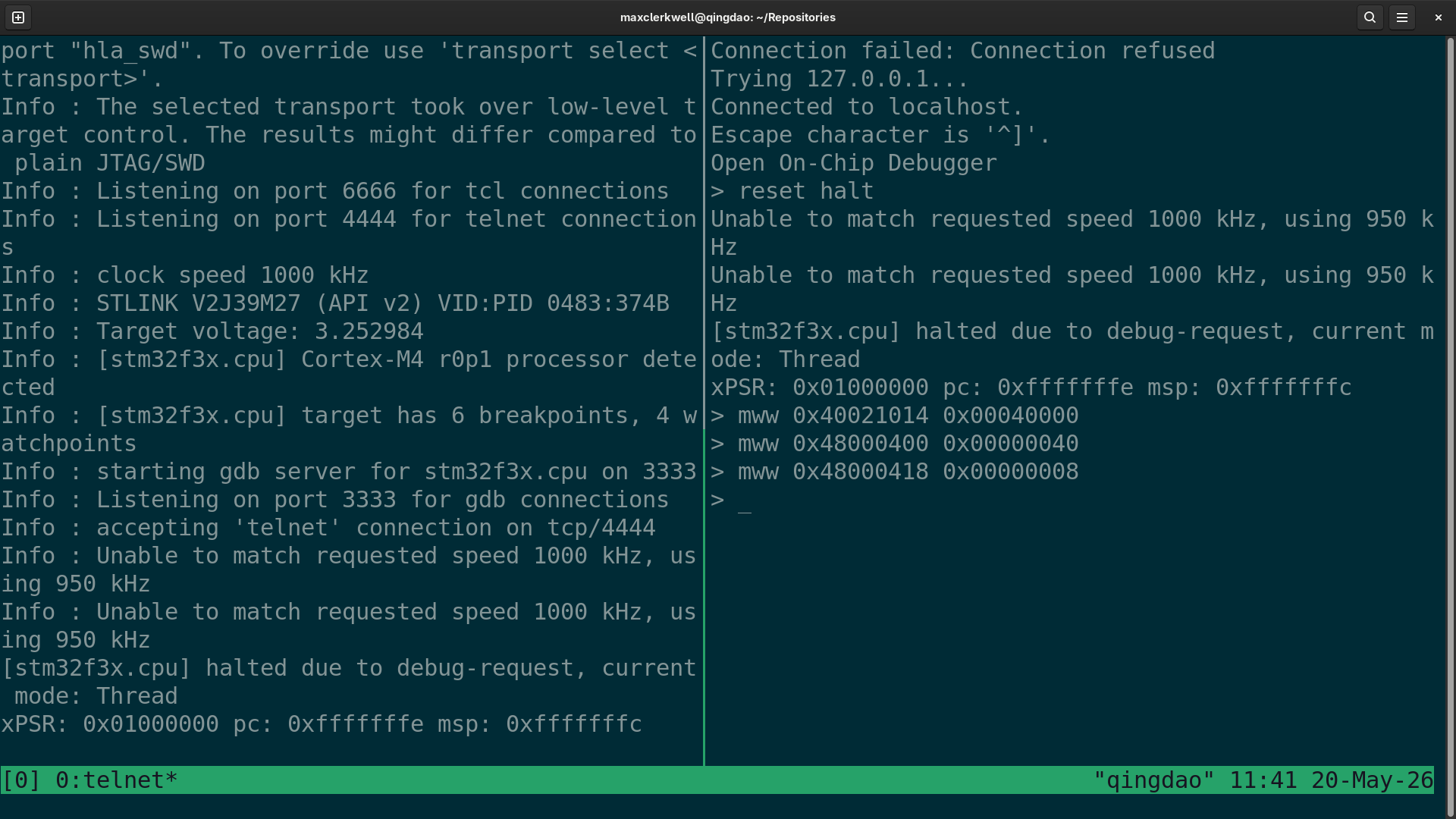
reset halt
mww 0x40021014 0x00040000
mww 0x48000400 0x00000040
mww 0x48000418 0x00000008
mww 0x48000418 0x00080000
Type those five lines one by one and watch LD3 respond.
Blinky — a small TCL loop
The telnet interface is a full TCL interpreter. after N pauses for N milliseconds. proc defines a procedure:
reset halt
mww 0x40021014 0x00040000
mww 0x48000400 0x00000040

proc blink {n} {
    for {set i 0} {$i < $n} {incr i} {
        mww 0x48000418 0x00000008
        after 500
        mww 0x48000418 0x00080000
        after 500
    }
}

blink 10
LD3 blinks ten times with a 500 ms period. No compiler, no linker, no flashing.
What Just Happened: SWD, Memory Mapping, and GPIO
The CPU was halted with reset halt. It executed zero instructions of firmware during the whole demo. Everything we did was OpenOCD writing directly to peripheral registers over SWD. The ST-Link bridge carried the writes from your terminal into the silicon.
This is the insight worth taking away: peripheral registers are memory. The GPIO, the RCC, the UART, the timers — they are all just addresses in the 32-bit address space. The CPU writes to them to configure hardware. You can write to them too, from outside the chip, using the debug interface that ARM put there precisely for this purpose.
Once you understand that, you understand what every line of your future bare-metal C code is actually doing.
Next steps
- Add a
USARTand send bytes the same way — no firmware needed. - Read
GPIOB_IDR(0x48000414) while pressing a button to watch the bit flip. - Write a TCL script and pipe it via
netcatfor non-interactive board tests. - When you are ready: write the same register sequence in C and flash it as a proper binary.
The reference manual is not a wall of intimidating text. It is a lookup table. You already know how to read it.