A Hill I Am Willing to Die On: HDL for PCB Netlists
This afternoon someone replied to one of my posts on X. The reply was from @blind_via and made the point that what I was describing already exists as a netlist, that schematics come from human creativity, and that removing humans from the loop leads to the same place as vibe coding. Fair points, all of them. But they did not change my mind.
What pushed me to write this out properly is something I keep hearing from people at university: AI will take a very long time to solve PCB design. Routing is too hard. Schematics require real engineering intuition. The problem is fundamentally different from software.
I disagree. Not because I think AI is magic, but because I think the problem is being misidentified.
Schematics Are Not the Ground Truth
I have written before about why PCB design should start with a block diagram, not a schematic. The argument there was about design intent: writing down what the board is supposed to do before reaching for KiCad. This post goes deeper into the toolchain.
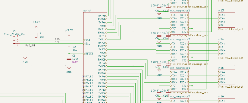
Here is the thing most people do not say out loud: a schematic is not the source of truth for a PCB. The netlist is. The schematic is a graphical interface that an engineer uses to construct the netlist. It is a drawing tool wrapped around a data format.
That data format encodes what actually matters: which pins are connected to which nets, which components are instantiated, what their parameters are. The schematic is how a human inputs that information. It is not the information itself.
This distinction matters enormously once you start thinking about AI, version control, and reuse.
The Abstraction Stack We Already Know
Physical hardware
^
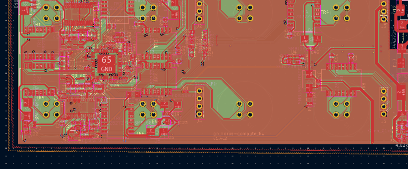
PCB layout <- routing, copper, keepouts
^
Netlist <- the actual source of truth
^
Schematic <- graphical interface to the netlist
^
Engineer <- you, drawing boxes and wires
Compare this to software. In the early days of computing, engineers wrote binary directly. Then assembler gave them a readable layer above the opcodes. Then C abstracted further, and C++ brought structures and reuse. Nobody writes production code in assembler today, not because assembler is wrong, but because working at that level of abstraction constantly is exhausting and error-prone.
PCB design is stuck somewhere between assembler and C. We are drawing schematics by hand and generating netlists from those drawings. That is the wrong direction. The netlist should be generated from a language, and the schematic should be a rendered output, a view, not the input.
This is not a new idea in hardware design. VHDL does exactly this for FPGAs: you write structured code, synthesize it, and the toolchain generates what the hardware should look like. I wrote about this workflow in Zero to One: VHDL and a Lattice iCEstick. The same principle should apply to regular PCB netlists.
Why This Is a Grammar Problem for AI
The claim that AI cannot handle PCB design usually focuses on routing, and routing is genuinely hard. Constraint satisfaction over a dense copper plane, thermal relief, differential pairs, impedance matching. That is a legitimately difficult spatial problem.
But schematics? Schematics are easier. And yet AI still produces garbage schematics. Why?
Because schematics are a visual grammar, and that grammar is implicit. The rules, what makes a schematic correct, readable, and reviewable, are not written down anywhere that a model can learn from cleanly. The netlist underneath has structure, but that structure is tangled up in coordinate data, symbol identifiers, and rendering metadata. It is not a clean language. It is a side effect of someone drawing something.
Here is the thing about Large Language Models: they are language models. That is the whole mechanism. They learn structure from structured text. If you give them a clean, typed, composable language for describing circuits, they have something they can actually learn from. If you give them a visual file format that encodes drawing positions alongside electrical connections, you are asking the model to extract meaning from noise.
If netlists were generated from a proper HDL, you would have a clean, learnable grammar. A model could be trained on that. More importantly, a human could write it with confidence, review it, test it, and version-control it properly.
That is the real reason AI struggles with schematics. It is not that circuits are too complex. It is that we have not given the domain a language worth learning from.
The Tools That Exist and Why They Frustrate Me
Some people have already tried to build this. I have played with several of them.
SKiDL is the most mature attempt. It lets you describe circuits in Python, assign components from KiCad libraries, define nets programmatically, and generate a netlist that KiCad can import. The concept is exactly right. The execution is where it falls apart. The toolchain is brittle. Library resolution breaks silently. Net names collide in ways that are hard to debug. Common failure modes I ran into, and that come up repeatedly in the community, include footprint lookup failures when library paths change between KiCad versions, SchLib import errors when component attributes do not match the expected schema, and netlist export producing empty or malformed output without any clear error message. Every session felt like fighting the scaffolding rather than describing a circuit. The project has slowed down significantly and KiCad 7/8 support is patchy.
Hdl21 takes a more principled approach. It is Python-native and focuses on analog circuits, with a clean module and instance model. The type system is stricter than SKiDL, which means more upfront discipline but fewer silent failures. The tradeoff is that it is less connected to real-world EDA toolchains: getting from an Hdl21 description to something you can hand to a PCB layout tool requires extra steps that are not yet well-documented.
JITX goes furthest in terms of ambition. It is a full DSL, not Python embedded, with its own compiler, constraint system, and layout integration. The ergonomics look impressive on paper, and it is next on my list to actually try. I cannot say more about it yet because I have not spent enough time with it.
None of these have hit the sweet spot yet. The concept is right. The implementations are still engineering prototypes, not tools you can confidently build a production board with.
What the Language Should Give You
Here is what a proper HDL for PCB netlists should make possible: things you cannot easily do with a schematic.
Parameterized instantiation. Imagine you need eight filter stages that share a topology but differ in cutoff frequency, component values, and multiplexer assignment. In a schematic, you draw this eight times. In a language, you write a filter module that takes parameters and instantiate it in a loop:
filters = [
    LowPassFilter(fc=1e3 * (i + 1), mux_channel=i)
    for i in range(8)
]
Each instance has distinct component values, meaningful net names, and a clear origin in the source. If you need a ninth filter, you change one number. If you need to change the topology, you change it once.
Reusable circuit blocks as libraries. A flyback converter topology, a USB ESD protection block, a current sense amplifier: these are things you should write once and import. Not copy-paste a schematic sheet. Import from a library, instantiate with parameters, done.
Diffable, reviewable source. This is the version control argument, and it is more specific than it sounds. KiCad stores schematics as S-expressions, a structured format in principle. In practice, every wire carries absolute canvas coordinates and a UUID. Move a component two millimetres to avoid an overlap and every wire connected to it changes. The diff is pages long. None of it tells you anything about the circuit.
Here is what a KiCad .kicad_sch file actually looks like for a handful of wires:
(wire (pts (xy 270.51 204.47) (xy 292.735 204.47))
  (stroke (width 0) (type default))
  (uuid 2ecffb78-f077-4f85-ab1b-26855ace0705)
)
(wire (pts (xy 212.725 72.39) (xy 256.54 72.39))
  (stroke (width 0) (type default))
  (uuid 2effec3a-4c6a-403c-b107-7839d0b5a154)
)
(wire (pts (xy 245.618 18.288) (xy 245.618 20.32))
  (stroke (width 0) (type default))
  (uuid 2fe92422-7d86-4186-8707-3628c538a251)
)
(wire (pts (xy 231.775 161.29) (xy 231.775 137.795))
  (stroke (width 0) (type default))
  (uuid 30b78f0e-1107-47f0-96ed-ab8a845bb7fa)
)
For comparison, here is what SKiDL generates as a netlist for a simple voltage divider:
(nets
  (net (code 1) (name "GND") (class "Default")
    (node (ref "C1") (pin "2") (pintype "PASSIVE"))
    (node (ref "R2") (pin "2") (pintype "PASSIVE")))
  (net (code 2) (name "MID") (class "Default")
    (node (ref "C1") (pin "1") (pintype "PASSIVE"))
    (node (ref "R1") (pin "2") (pintype "PASSIVE"))
    (node (ref "R2") (pin "1") (pintype "PASSIVE")))
  (net (code 3) (name "VCC") (class "Default")
    (node (ref "R1") (pin "1") (pintype "PASSIVE"))))
No coordinates. No UUIDs. Just which pins are connected to which nets. That is closer to what matters. But to be clear: this netlist is still not what belongs in version control. It is an artifact, generated from the source. What belongs in version control is the Python file that produced it, the actual language description of the circuit. The netlist is the output of a compiler, not the input to one. That distinction is exactly the point.
The Open Question: Rendering
There is one problem I do not have a clean answer to yet, and I want to name it honestly rather than paper over it.
If the netlist is the source and the schematic is a rendered view, something has to decide where each block goes on that view. Automatic layout algorithms for graphs are notoriously difficult to control. Anyone who has used Mermaid or PlantUML for anything non-trivial knows the frustration of a box ending up on the wrong side of the diagram with crossing arrows everywhere.
A good schematic has intentional topology: power rails at the top, ground at the bottom, signal flow left to right, related subcircuits clustered together. That spatial intent is hard to encode in a language and hard to infer from a netlist.
I think this is a solvable problem. Layout hints in the source, constraint-based placement, interactive adjustment of a generated layout. But I have not found a satisfying solution yet, and I am not going to pretend I have. This is the thing I am still thinking about and it will probably be its own post.
Where This Leaves AI
Routing is hard. I will grant that. But the reason AI cannot yet generate useful schematics is not that circuits are beyond its reach. It is that we have not given the domain a language worth learning from.
Large Language Models learn language. That is the mechanism. Give a model a clean grammar with consistent structure and enough examples, and it learns the grammar. That is not a controversial claim. It is how these systems work. The absence of a proper HDL for PCB netlists is not just a tooling problem for humans. It is a structural reason why AI cannot make progress on schematic generation. Fix the language layer, and the picture changes.
That is why I disagree with the “AI will take a very long time” crowd: not because routing is easy, but because the bottleneck is not intelligence. It is grammar.
If you have thoughts on this, find me on X and reply: @maxclerkwell.